

 17. September 2026
 From Lab Concept to Serial Production: Addressing the PIC Polishing Challenge with KrellTech NOVA
Why repeatable component loading is the first hurdle
Every polishing process depends on how reliably a chip is loaded and secured. Repeatability in loading directly affects polishing uniformity, particularly at micron-scale tolerances. The difficulty is not only holding the chip securely, but referencing it to a common datum point, especially when incoming chips already show inconsistencies from upstream fabrication such as non-parallel edges, uneven widths, or excess epoxy from layered assemblies.
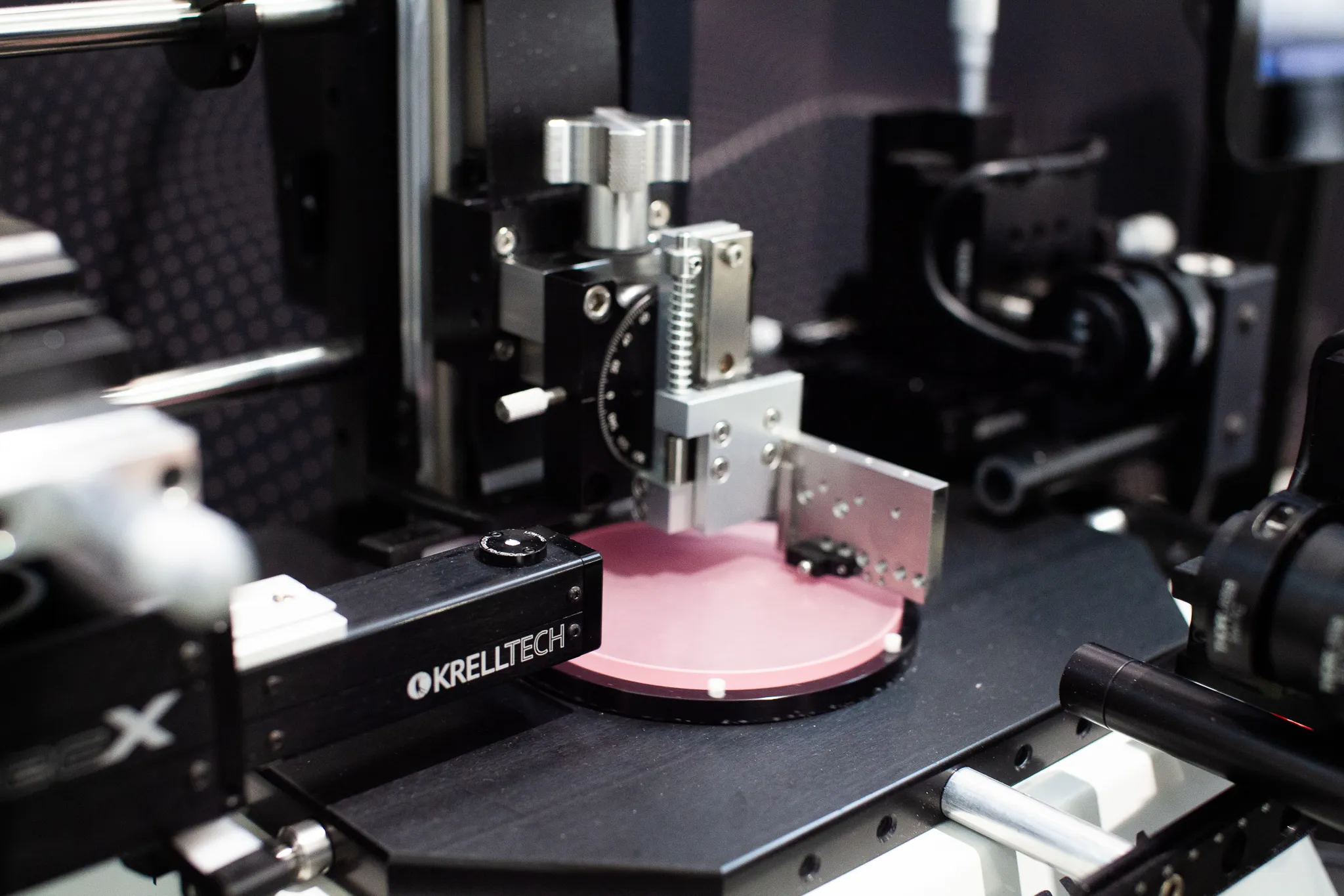
NOVA addresses this with adjustable fixtures that accommodate varying chip dimensions while keeping clamp forces away from critical optical areas. Clamp materials are selected to be non-abrasive, and force is applied in opposing directions to prevent rotation or lifting during polishing. For very small chips, an off-line carrier-based loading method with video-assisted referencing supports micron-level placement accuracy and removes technician-to-technician variability from the process.

Polishing determines the final optical and geometric quality of a photonic integrated circuit (PIC), but it is often treated as a secondary step during development. As a process scales from a validated lab setup to volume production, die-cut variation, fixture alignment and throughput requirements start to limit yield in ways the original process was not built to handle.
This is a familiar situation for OEMs and research institutions working with silicon photonics, lithium niobate, indium phosphide, and other PIC materials. AMS Technologies supports these customers with the KrellTech NOVA™, a modular polishing platform built to carry a process from development through volume manufacturing without a full process redesign along the way.
Fixture design and calibration as the foundation of precision
For PICs that require variable endface angles or multiple facets on a single edge, the fixture needs to allow rotation and angular control without removing the sample, which calls for both flexibility and stability in how it is held.
NOVA uses active calibration against a reference sample, monitored over an interferometric plane, to align the fixture to the polishing surface. This active approach avoids the limits of passive, machined alignment. An independent suspension system keeps contact pressure between the chip and the polishing film consistent as material is removed, preventing chatter and vibration while letting the fixture ride the z-axis on a linear slide under a precision-tuned spring.

Process control at the micron level, across materials
PICs are sensitive to stress and thermal buildup, which makes conventional polishing systems ill-suited to the task. NOVA introduces programmable descent control with micron-level positioning: rather than applying full pressure on contact, the chip is advanced incrementally to the polishing film, reducing the risk of edge chipping or over-polishing and giving fine control over material removal.
An integrated video inspection module lets the operator monitor polishing in progress and check endface geometry and material removal without removing the chip, which reduces scrap and handling risk, particularly useful during process development when fast iteration matters. Because PIC materials vary widely, from silicon and silicon nitride to lithium niobate and indium phosphide, NOVA supports multi-step processes across a range of abrasive films, including silicon carbide, aluminum oxide, diamond, and silicon dioxide. Each polishing cycle can be adjusted in real time during development and then saved as a repeatable program for volume manufacturing, covering pressure, speed, cycle time, and abrasive film selection.
One platform, from single-position development to multi-position production
Many polishing platforms are built for either R&D or production, and few carry a process across that transition without disruption. NOVA is modular by design: customers can start with a single-position workholder for process development and add positions later for volume production, with each position retaining the suspension mechanism that compensates for individual chip loading variation.
NOVA’s Android-based software further simplifies training and process transfer. Step-by-step prompts let less experienced technicians reproduce complex polishing sequences, supporting consistent results across operators and shifts. The system is not limited to PIC chips: its interchangeable fixture system also supports fiber arrays, shaped bare fibers, and terminated components, so a single platform can cover most of a customer’s photonic component polishing needs.
What AMS Technologies adds to the NOVA system
Selecting and installing polishing equipment is only part of the task. AMS Technologies supplies the KrellTech NOVA together with hands-on consultation to configure and optimize the system for the customer’s own production process, from fixture and abrasive selection to the transition from a single R&D position to a multi-position production setup.
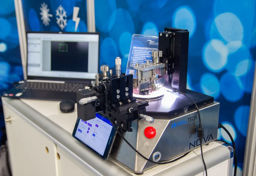
This reflects how AMS Technologies works with OEMs more broadly: as one partner across component selection, integration, and production support, rather than a supplier of equipment alone. Our own NOVA demonstration unit illustrates the build quality behind the system: in use for over ten years and well-traveled across customer sites and trade shows, it still runs without issue, alongside a number of satisfied customers who use NOVA in their own production today.
What’s next
Are you evaluating how to take a PIC polishing process from development into volume production? Contact our technical experts to discuss your requirements, or request a demonstration of the KrellTech NOVA modular polishing system.
Read more about Fiber Optics Processing and Qualification

FAQ: Krell NOVA Modular Polishing System
What is the NOVA Workcell System?
NOVA from KrellTech is a modular polishing platform for photonic components. It combines precision polishing, configurable fixtures, micron-level positioning, process control, and in-line inspection.
Can NOVA be used for both PIC development and production?
Yes. NOVA can be configured with a single-position workholder for process development and later expanded with multi-position fixtures for higher-throughput production. Developed polishing processes can be saved and transferred to production.
How does NOVA accommodate variations between individual PICs?
Adjustable fixtures accommodate variations in chip dimensions, while an independent suspension system helps compensate for differences in component loading and maintain consistent contact pressure during polishing.
Which PIC materials can be polished with NOVA?
NOVA supports multi-step polishing processes for materials including silica, silicon nitride, lithium niobate, and indium phosphide. Different abrasive films can be selected according to the material and process requirements.
How does NOVA help control material removal during PIC polishing?
Programmable descent control with micron-level positioning allows the component to approach the polishing film incrementally. Together with controlled pressure, speed, and cycle time, this enables precise control over material removal and helps reduce the risk of edge chipping or over-polishing.
Can components be inspected during the polishing process?
Yes. Integrated video inspection allows operators to monitor polishing progress and inspect the component without removing it from the system. This reduces additional handling and allows endface geometry and material removal to be checked during the process.
What support does AMS Technologies provide for PIC polishing applications?
AMS Technologies looks at the polishing system in the context of the customer’s overall production process. We review components, materials, handling, process steps, and production requirements, identify potential improvements, and recommend a suitable system configuration and process.
EXPLORE MORE
NEWS & EVENTS
AMS Technologies and neoLASE join B2Run Hannover
B2Run Hanover 2026 was fun! Thank you to EPIC Photonics, the organizing team – and most of all to our runners from AMS Technologies and ...
Read More >

Boosting FLIM for Next-Generation Cancer Diagnostics
Cancers developing in epithelial tissues lining account for a large share of new cancer cases worldwide – and consequently to cancer-related deaths. (1) Early and ...
Read More >
AIMEN Laser Week
October 26–29, 2026
O Porriño, ES
AIMEN Laser Week is an international event dedicated to laser technologies and their applications in industrial manufacturing, process monitoring, and analytical systems. The conference combines ...
Read More >
