

 20. Oktober 2026
From Prototype to Product: Photonic Packaging at Bay Photonics

A photonic device that works on an optical bench is not yet a finished product. Packaging determines whether the optical alignment holds, whether heat leaves the chip, whether the device is protected from moisture, and whether the design can be built again with the same result. For many OEMs and research institutions, this is where projects slow down: packaging requires specialized equipment, process know-how and experienced people, and few providers in Europe offer all three for small volumes and changing designs.
Since April 2026, Bay Photonics in Paignton, UK, has been part of AMS Technologies. Its team assembles and packages VCSELs, edge-emitting lasers, photodiodes, sensors and hybrid photonic integrated circuits (PICs) for telecom, quantum technologies, defense, medical and space applications. This article looks at the problems customers bring to Paignton and how the team solves them.
Keeping the alignment stable after assembly
Coupling light between a laser, a PIC and a fiber often requires sub-micron alignment. Reaching that position once is not the difficult part. The alignment also has to hold while the adhesive cures, through temperature changes and over the life of the device.
Bay Photonics aligns single fibers, fiber arrays and micro-optics on sub-micron workstations, using active alignment with optical feedback where the coupling tolerance requires it. The coupling method follows the device: direct butt-coupling with index-matching adhesive for edge-emitting lasers and detectors, lensed fibers for free-space coupling, and grating coupling for silicon photonic PICs. For devices that are sealed or operated in vacuum, as is common in quantum and space applications, the team uses low-outgassing adhesives to keep contamination away from optical surfaces.
Getting heat out and keeping moisture away
Lasers in particular are sensitive to how well heat leaves the chip. Voids in a solder joint weaken the thermal path and the mechanical bond, and they are not visible from the outside. Moisture and contamination inside a package degrade optical and electrical performance over time.
Bay Photonics addresses both. Eutectic and solder die attach with vacuum processing produce void-free joints, and X-ray tomography checks bonds and joints non-destructively. Where temperature control is needed, the team integrates TECs and thermistors into gold-plated Kovar enclosures. Hermetic sealing by resistive seam welding or projection welding closes TO cans, gold boxes and custom metal or ceramic housings. Fine and gross leak testing and residual gas analysis then verify the seal, and qualification to Telcordia and MIL-STD requirements supports customers in telecom, space and defense.

Carrying a prototype process into production
A packaging process developed by hand on a few prototypes often does not transfer directly to production. Parameters change, fixtures are missing, and test steps were never defined.
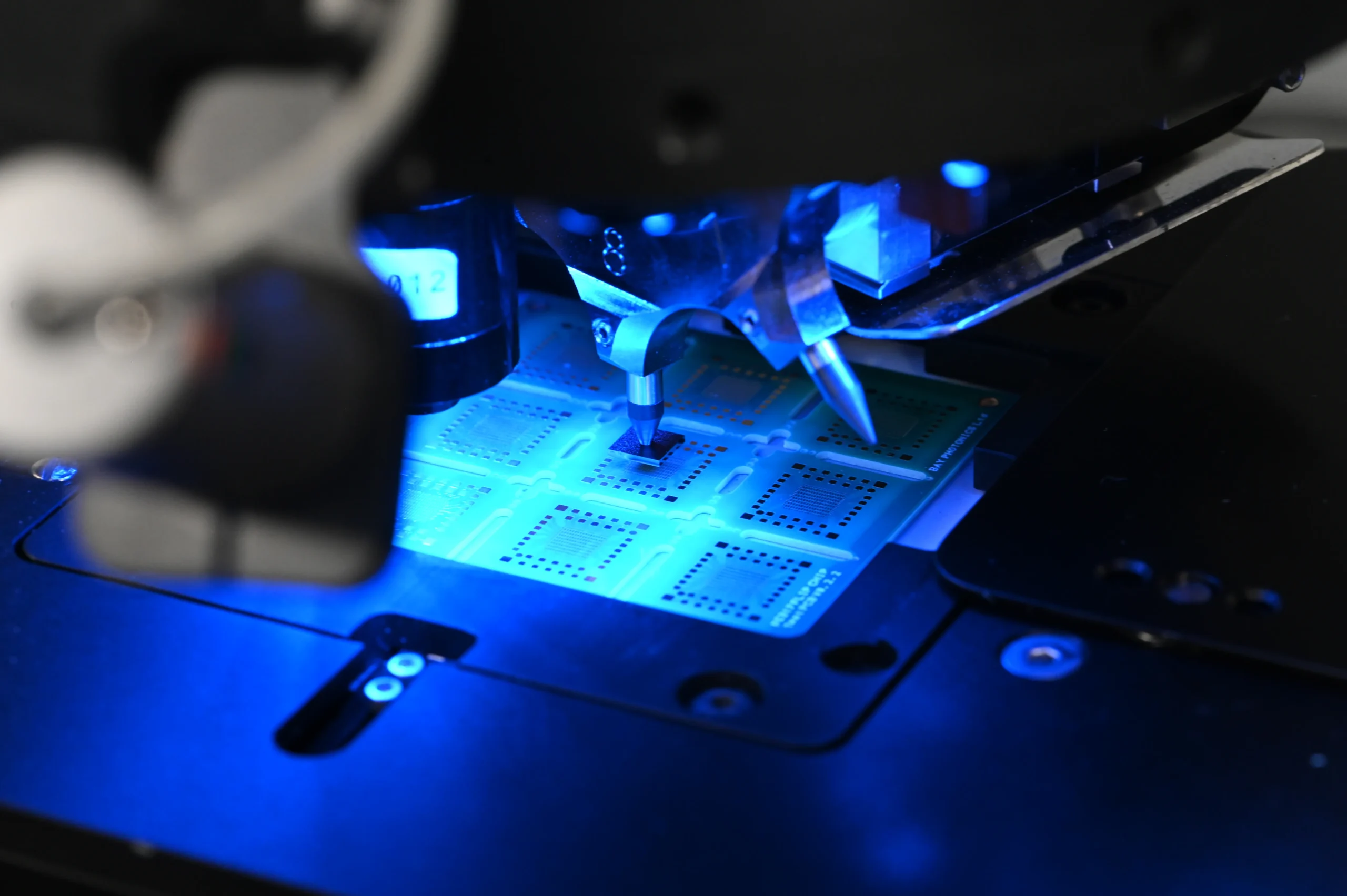
Bay Photonics uses semi-automatic die bonders for prototype builds and parameter optimization, and fully automated die bonding once a design moves toward higher volumes. The parameters found on the prototype are carried into production instead of being developed twice. In wire and ribbon bonding, the team controls bonding force, ultrasonic energy, time and loop profile with in-process monitoring, which makes results repeatable from build to build. Support for Design for Manufacturing (DFM), Design for Test (DFT) and New Product Introduction (NPI) brings manufacturing and test requirements into the design before they become expensive to change.
Partner for small volumes and changing designs
High-volume packaging lines are built for stable designs and large quantities. Projects with varying designs, frequent changes and smaller batches often do not fit them.
The Paignton site is set up for this kind of work. Its in-house design team considers optical, RF, mechanical, thermal and environmental performance together, and the team builds both standard and custom packages. Customers can bring a single process step, such as wire bonding or hermetic sealing, or a complete module that combines thermal control, electronics and free-space or fiber optics. The site operates cleanroom and precision assembly facilities and is certified to ISO 9001:2015 and ISO 14001:2015.

Where the know-how comes from
Paignton has a long history in photonics manufacturing. In the late 1990s, Nortel Networks produced tens of thousands of hermetically sealed lasers, detectors and modulators per week at its Paignton site, for fiber networks that had to run for decades, often in remote locations. In the early 2000s, this manufacturing moved to Southeast Asia, and with it much of the specialized knowledge built up in the region.
Bay Photonics was founded in 2007 by two former Nortel engineers. Starting with a small team and second-hand equipment, they continued to build fixtures, train staff and package devices. Demand from quantum technologies helped the company grow substantially from 2020 on. Today, Bay Photonics has 33 employees and works from the Electronics and Photonics Innovation Centre (EPIC) in Paignton, which was built to support new high-tech companies in the area.

Passing the know-how on
OEM products in markets such as medical, space or defense often stay in production for many years, and redesigns and follow-up generations need the same packaging know-how as the original. That know-how is learned largely through practice: tooling, sealing, alignment and debugging thermomechanical problems take time to master. With the growing shortage of skilled engineers in our industry, it only stays available if the next generation is trained now.
Bay Photonics does this in several ways. Around 15% of the team are apprentices, the company has a close partnership with South Devon College, and it is part of the engineering community around the EPIC Centre and the Torbay Hi-Tech Cluster.

Part of AMS Technologies
Packaging is one step in a longer path. Before it comes component selection, optical design, thermal management and electronics. After it comes integration into a system, production and supply over the product’s lifecycle. Each step affects the others: the optical design defines the coupling, the thermal design defines die attach and temperature control, and the electronics define the bonding. When different suppliers handle these steps, interface problems often appear only at assembly.
AMS Technologies supports customers along this whole path, from feasibility through prototype and production to lifecycle management. We select components from our network of qualified manufacturers, develop optical, thermal and electronic designs, and integrate and produce custom solutions at our sites in Hanover and Kraków. Bay Photonics adds photonic device packaging to this chain. Customers can move from a component or concept to a packaged device and on to a complete system, with one partner coordinating the interfaces.
Customers can also use individual steps, such as packaging alone, or transfer complete work packages. All three sites are in Europe, close to customers’ engineering, quality and supply chain teams, which shortens feedback loops and keeps critical know-how in Europe.

What’s next?
Are you taking a photonic device from prototype to production, or looking for packaging capacity in Europe? Contact our technical experts to discuss your requirements.
Get Inspired

From Lab Concept to Serial Production: Addressing the PIC Polishing Challenge with KrellTech NOVA
Read More >
Efficient Subcontracting in Europe: Expanding HMLV Capabilities
Read More >
Five Situations Where High-Tech Companies Benefit from External Production Support
Read More >
Press Release: AMS Technologies AG Acquires Bay Photonics Ltd. to Expand Photonics Packaging Capabilities
Read More >
Press Release: AMS Technologies and VIAVI Solutions expand their partnership to include measurement technologies for Photonics Integrated Circuits (PICs)
Read More >FAQ: Photonic packaging at Bay Photonics
What photonic packaging services does Bay Photonics provide?
Bay Photonics covers die attach, wire and ribbon bonding, optical alignment and coupling, hermetic sealing, and optical, electrical and environmental testing. Its in-house design team also supports package design, Design for Manufacturing (DFM), Design for Test (DFT) and New Product Introduction (NPI).
Which devices and applications does Bay Photonics support?
The team packages VCSELs, edge-emitting lasers, photodiodes, sensors and hybrid photonic integrated circuits (PICs). Typical applications are in telecom, quantum technologies, defense, medical and space.
Does Bay Photonics take on prototypes and small batches?
Yes. The site is set up for prototypes, qualification batches, small batches and high-mix, low-volume production, including devices with special requirements. The process follows the design and can change from build to build.
Can we use individual process steps instead of outsourcing the complete package?
Yes. Customers can bring a single step, such as wire bonding or hermetic sealing, or a complete module that combines thermal control, electronics and free-space or fiber optics. Bay Photonics builds both standard and custom packages.
Which hermetic packages and sealing methods are available?
Bay Photonics seals TO cans, gold-plated Kovar enclosures (gold boxes) and custom metal or ceramic housings. Sealing methods are resistive seam welding and projection welding. Gold boxes can include TECs and thermistors for temperature control.
How is package quality verified?
Testing includes X-ray tomography for voids and bond defects, die shear and wire pull testing, fine and gross leak testing, residual gas analysis, and environmental testing. Bay Photonics also supports qualification to Telcordia and MIL-STD requirements.
How does Bay Photonics support the transition from prototype to production?
Prototype builds and parameter optimization run on semi-automatic die bonders, and fully automated die bonding is available once a design moves toward higher volumes. Parameters found on the prototype are carried into production, and DFM and DFT support brings manufacturing and test requirements into the design early.
How does Bay Photonics work with the other AMS Technologies sites?
Since April 2026, Bay Photonics has been part of AMS Technologies. Packaging can be planned together with optical design and laser systems in Hanover and with thermal management, electronics and subcontract manufacturing in Kraków, with one partner coordinating the work. All three sites are in Europe.
EXPLORE MORE
NEWS & EVENTS
AMS Technologies and neoLASE join B2Run Hannover
B2Run Hanover 2026 was fun! Thank you to EPIC Photonics, the organizing team – and most of all to our runners from AMS Technologies and ...
Read More >

From Lab Concept to Serial Production: Addressing the PIC Polishing Challenge with KrellTech NOVA
Why repeatable component loading is the first hurdle Every polishing process depends on how reliably a chip is loaded and secured. Repeatability in loading directly ...
Read More >

AIMEN Laser Week
October 26–29, 2026
O Porriño, ES
AIMEN Laser Week is an international event dedicated to laser technologies and their applications in industrial manufacturing, process monitoring, and analytical systems. The conference combines ...
Read More >
